|
NOVIDADES
Popular in electronic devices including solar panels, silicon has its limits. Scientists are devising replacements to meet the technology demands of an energy-hungry nation. A team of researchers devised a new method to grow atomically thin films of a promising group of materials, known as hybrid perovskites ("Atomically thin two-dimensional organic-inorganic hybrid perovskites"). The material grew in well-defined, relatively large squares. For the first time, researchers have introduced an ionic semiconductor to the family of two-dimensional (2D) nanomaterials. As an ionic material, it has special properties that graphene and other 2D nanomaterials don’t have. 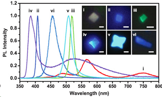 Scientists made a promising material for photovoltaics into atomically thin sheets that could be used for new solar panels and many other electronic applications. The material is a hybrid organic-inorganic halide perovskite. To make the thin sheets, scientists grew crystals from a chemical solution, resulting in a well-defined shape and a large lateral dimension (as shown in the inset images). These atomically thin, 2D hybrid perovskite sheets emit light (labeled as PL (photoluminescence) Intensity in the graph) whose color (wavelength) is tunable by changing sheet thickness and composition (i through vi). (© AAAS) This study introduces a potential successor to silicon. This new family of materials, called planar hybrid perovskites, could lead to advanced solar cells, light-emitting electronics, photodetectors, and other optoelectronic devices. In addition, this study shows a way to manufacture these atomically thin semiconducting materials. Scientists created a new form of hybrid organic-inorganic perovskites in atomically thin 2D sheets. These hybrid perovskites have shown promise as semiconductor materials for photovoltaic applications. This new 2D material could provide an alternative to other 2D semiconductors that are widely studied as potential successors to silicon in future electronic devices. In other words, hybrid perovskite sheets could be an alternative to graphene, boron nitride, and molybdenum disulfide in future electronics. Scientists grew the hybrid perovskite sheets from solution, yielding single layer and few-unit-cell-thick crystals. The thin crystals had a well-defined square shape and a relatively large lateral dimension (up to 10 micrometers). Unlike other 2D materials, the hybrid perovskite sheets have an unusual atomic-scale structural relaxation. Advantageously, this subtle structural change in the 2D material led to a noticeable shift in the electronic band gap. This shift in the band gap did not occur in the bulk (3D) crystal of the same material. Researchers discovered that the new 2D crystals produce efficient photoluminescence and that color tuning of the emitted light could be achieved by changing the sheet thickness and composition. This study opens up opportunities for fundamental research into thin 2D hybrid perovskites and introduces a new family of 2D semiconductors for potential applications in advanced optoelectronic devices. Lawrence Berkeley National Laboratory, Posted: Jul 27, 2016. |
|||||||||||||||||||||||||