|
NOVIDADES
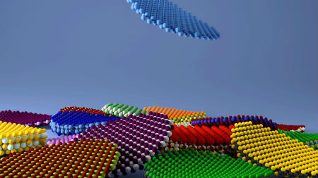 EPFL scientists identified more than 1000 2D materials. Credit: EPFL/G.Pizzi
"To find other materials with similar properties, we focused on the feasibility of exfoliation,” explains Nicolas Mounet, a researcher in the THEOS lab and lead author of the study. "But instead of placing adhesive strips on graphite to see if the layers peeled off, like the Nobel Prize winners did, we used a digital method." To build their database, the researchers used a step-by-step process of elimination. First, they identified all of the materials that are made up of separate layers. "We then studied the chemistry of these materials in greater detail and calculated the energy that would be needed to separate the layers, focusing primarily on materials where interactions between atoms of different layers are weak, something known as Van der Waals bonding," says Marco Gibertini, a researcher at THEOS and the second author of the study. "Our study demonstrates that digital techniques can really boost discoveries of new materials," says Nicola Marzari, the director of NCCR MARVEL and a professor at THEOS. "In the past, chemists had to start from scratch and just keep trying different things, which required hours of lab work and a certain amount of luck. With our approach, we can avoid this long, frustrating process because we have a tool that can single out the materials that are worth studying further, allowing us to conduct more focused research." It is also possible to reproduce the researchers' calculations thanks to their software AiiDA, which describes the calculation process for each material discovered in the form of workflows and stores the full provenance of each stage of the calculation. "Without AiiDA, it would have been very difficult to combine and process different types of data," explains Giovanni Pizzi, a senior researcher at THEOS and co-author of the study. "Our workflows are available to the public, so anyone in the world can reproduce our calculations and apply them to any material to find out if it can be exfoliated." By Sara Perrin. École Polytechnique Fédérale de Lausanne (EPFL). Posted: Mar 06, 2018. Nota do Manager Editor: A publicação que deu origem a esta notícia de título: "Two-dimensional materials from high-throughput computational exfoliation of experimentally known compounds" de autoria de N. Mounet, M. Gibertini, P. Schwaller, D. Campi, A. Merkys, A. Marrazzo, T. Sohier, I. E. Castelli, A. Cepellotti, G. Pizzi and N. Marzari, foi publicada no periódico Nature Nanotechnology (2018), DOI: 10.1038/s41565-017-0035-5. Assuntos Conexos: The intriguing properties and nanotechnology applications of graphene and graphene analogs. |
|||||||||||||||||||||||||