|
NOVIDADES
Metals are usually characterized by good electrical conductivity. This applies in particular to gold and silver. However, researchers from the Max Planck Institute for Solid State Research in Stuttgart, together with partners in Pisa and Lund, have now discovered that some precious metals lose this property if they are thin enough. The extreme of a layer only one atom thick thus behaves like a semiconductor. This once again demonstrates that electrons behave differently in the two-dimensional layer of a material than in three-dimensional structures. The new properties could potentially lead to applications, for example in microelectronics and sensor technology. One might think that gold leaf, which is only 0.1 µm thick, is actually quite thin. Far from it. It can actually be several hundred times thinner. For example, the research team of Ulrich Starke and his former doctoral student Stiven Forti have successfully created a gold layer only a single atom thick. Two-dimensional gold, so to speak. 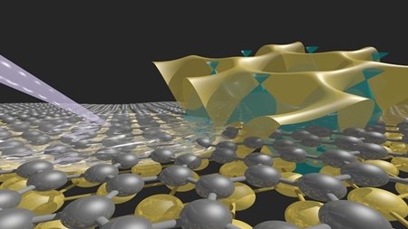 Sandwich with electronic spice: The illustration shows a crystalline monoatomic gold layer under graphene (anthracite). The electronic structure of the gold layer and the graphene (green) is shown above. The Stuttgart Max Planck researchers spectroscopically determined the electronic properties by examining the sample with a photon beam (grey). Credit: Stiven Forti
The team had also applied the intercalation technique to other elements, including germanium, copper, and gadolinium. Yet, according to Forti, the main focus was the influence on the properties of graphene. In the case of gold, however, it was found for the first time that the intercalated atoms arranged themselves in a regular, periodically recurring two-dimensional structure — crystalline—along the silicon carbide surface. "If the intercalation is carried out at 600°C, the graphene layer prevents the gold atoms from agglomerating to form drops", says Forti about the function of the carbon layer in the sandwich structure. 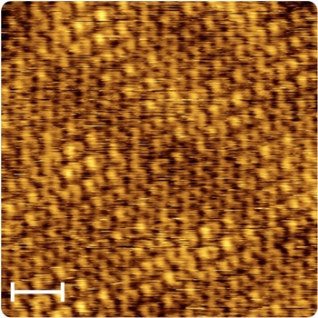 Hint at hidden precious metal: The image of a scanning tunnelling microscope shows graphene under which there is a crystalline gold layer a single atom thick. In addition to the hexagonal structure of the graphene, fluctuations in brightness can be seen in the image. These arise because the gold layer interacts with the graphene and forms a superlattice, the Moiré lattice. The scale bar represents one nanometer. Credit: © MPI for Solid State Research
Semiconductors are essential materials in microelectronics and other fields. For example, electronic switching elements such as diodes or transistors are based on it. Starke's team can envisage some typical semiconductor applications for the new 2-D material. A second layer of gold atoms again gives a metallic character—and thus influences the electrical conductivity. "By varying the amount of sublimated gold, we can tightly control whether one or two layers of gold form", explains Forti. It would therefore be conceivable to use components with alternating single- or double-atomic gold layers. The new manufacturing method would then have to be suitably combined with common lithographic methods of chip production. For example, diodes significantly smaller than conventional ones could be produced. According to Starke, the different electronic states of single and double-layer gold could also be used in optical sensors. Starke's team has already taken the next step in the production of two-dimensional precious metal layers. Also in an intercalation experiment with silver, a strictly crystalline two-dimensional silver layer formed between silicon carbide and graphene. And what's more: even this metal, which is usually an even better electrical conductor than gold, becomes a semiconductor when reduced to two dimensions. The initial results indicate that the energy required to make the silver layer electrically conductive is probably higher than for 2-D gold. "The semiconductor properties of a component made from this material might therefore be thermally more stable than those of gold", says Starke about possible practical consequences. Philipp Rosenzweig et al. Large-area synthesis of a semiconducting silver monolayer via intercalation of epitaxial graphene, Physical Review B (2020). DOI: 10.1103/PhysRevB.101.201407
|
|||||||||||||||||||||||||