|
NOVIDADES
Recently, organic-inorganic hybrid perovskites ABX3 (A=organic molecules; B=Pb2+ or Sn2+; and X=Cl-, I-, and/or Br-)) have received increasing research attention owing to their impressive optoelectronic properties and high performance in photovoltaic devices with the power conversion efficiency over 20%. These materials exhibit many interesting properties such as intrinsic ambipolar transport, high optical absorption coefficient, tunable bandgap, high quantum efficiency and long carrier diffusion length, showing promising potential for optoelectronic devices such as solar cells, photodetectors, as well as light-emitting diodes. Perovskites CH3NH3PbX3 (X=Cl, Br, or I) can be considered as two-dimensional (2D) layered structures and they exhibit strong quantum confinements in reduced dimensions (numbers of layers). So, it is intriguing to explore the optoelectronic properties of perovskites when reducing the thickness into a few atomic layers at which they shows quantum confinement effects. Meanwhile, the realization of 2D perovskite with controllable thickness (less than 10 nm) even single unit cell thickness will contribute to the better understanding of the intrinsic optoelectronic properties, charge carrier characters and the development of perovskite based functional devices. A variety of methods have been developed to synthesize both colloidal as well as thin films of CH3NH3PbX3 perovskite materials from polycrystalline film to bulk single crystal. However, the introduction of defects and grain boundaries in perovskite is unavoidable, which could influence the optoelectronic properties. Additionally, it is expected that the perovskite will exhibit unique properties after reducing it into few- or single-unit-cell thickness crystal since that the 2D quantum wells are exposed and the electronic coupling between top and bottom layers may be varied. However, an important issue need to be addressed is that perovskites can obtain different dimensionalities based on component sizes. Occupation of A sites by monovalent cations, such as CH3NH3+ and HC(NH2)2+, form a 3D framework, whereas if a larger cation, such as CH3CH2NH3+, is used, 2D or 1D structures can be obtained. In this regard, It is extremely challenging to synthesize ultrathin 2D CH3NH3PbX3 perovskite with a thickness down to a single unit cell because of the intrinsically non-van der Waals-type 3D characteristics. 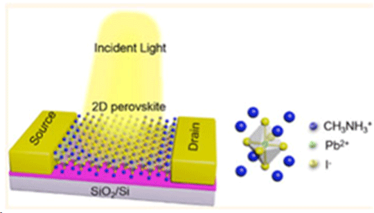 Schematic illustration of photodetector based on 2D CH3NH3PbI3. A research team lead by Bao et al. at Soochow University demonstrated the world’s thinnest CH3NH3PbI3 perovskite nanosheets by a two-step synthesis method through the combination of solution process to produce 2D PbI2 nanosheets and vapour-phase conversion of the PbI2 to CH3NH3PbI3 nanosheets. This research was published in ACS Nano on 24th February ("Two-Dimensional CH3NH3PbI3 Perovskite: Synthesis and Optoelectronic Application"). The prepared high quality nanosheets with triangle and hexagonal shapes can be as thin as a single unit cell (~1.3 nm). They also shows tunable photoluminescence while the thickness or composition is changed. Thanks to its high quantum efficiency and excellent photoelectric properties, a high-performance photodetector was demonstrated. The device not only shows greatly enhanced photo responsivity (23 AW-1) and an ultra-fast response (< 20 ms), but also has the capability for broadband photodetection from the ultraviolet to the entire visible spectral range. Furthermore, they also experimentally demonstrated the fabrication of in-plane 2D pervoskite heterostucture, which may find interesting applications for light emission diodes. 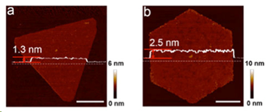 (a-b) AFM topography images of 2D CH3NH3PbI3 nanosheets with different thicknesses. Scale bars: 2 µm. This synthesis approach allows the researchers to investigate the exact correlation between the number of layers in perovskites and their optoelectronic properties. This approach could be extended to the perovskites made of different halide ions with different compositions, stated by Dr. Bao. Moreover, it will be highly important to tune the optical properties of perovskites across the whole visible spectrum. This pioneering work on low-dimensional perovskites is an important milestone not only for the fundamental understanding of the hybrid perovskites family, but also for their new applications in optoelectronics. This work has far-ranging impact and will stimulate interest in several communities, e.g. synthesis and characterization of low-dimensional other hybrid organic-inorganic perovskites, development of perovskite-based photonics and optoelectronics with wavelength tunability, concluded Dr. Qiaoliang Bao. Source: Monash University. Posted: Mar 16, 2016. |
|||||||||||||||||||||||||