|
NOVIDADES
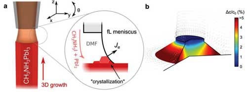
Organic–inorganic metal halide perovskites have emerged as a promising optoelectronic material with exceptional structure and property tunability. This new generation of functional materials possess excellent properties such as large optical absorption, long carrier diffusion length, high carrier mobility, and low-cost solution production process. The research attention in metal halide perovskites has grown exponentially since 2009, when the use of organometal halide perovskites as visible-light sensitizers for photovoltaic cells was reported (JACS, "Organometal Halide Perovskites as Visible-Light Sensitizers for Photovoltaic Cells"). In the decade since, a rapidly growing body of research has utilized perovskites for applications as solar cells, photodetectors, light emitting diodes, and lasers. In recent years, structure control of organic–inorganic metal halide hybrids has been explored to lower the dimensionality from 3D to 2D, 1D, and 0D at both morphological and molecular levels (see for instance: "Ultrathin perovskite nanocrystals suitable for use in tunable and energy-efficient LEDs" or work on light-emitting nanoantennas based on halide perovskites). At the same time, fabrication methods based on inkjet printing emerged for patterning such perovskite micro- and nanostructures. However, these patterning techniques for perovskites are still limited to in-plane fabrication and alignment. To overcome this limitation, researchers have developed a method to print perovskite nanostructures in three dimensions. The method exploits a femtoliter meniscus of precursor ink formed on a nanopipette to localize and guide solution-mediated perovskite crystallization in mid-air, enabling nanoscale and freeform 3D printing. The researchers, led by a team from the Department of Mechanical Engineering at The University of Hong Kong, have published their findings in Advanced Materials ("3D Nanoprinting of Perovskites").  Perovskite 3D printing. a) Schematic illustration showing meniscus-guided 3D printing of organic–inorganic metal halide perovskites. Crystallization of CH3NH3PbI3 occurs at a confined femtoliter (fL) ink meniscus and its continuous guiding process enables nanoscale 3D printing. Inset: Evaporative loss of solvent (Je: the evaporation flux of solvent) increases the solute concentration at the surface of the meniscus, promoting perovskite crystallization. b) The computed concentration of perovskite solutes inside the meniscus (height: 250 nm; wetting diameter: 1160 nm), forming a rim-shaped concentration field. The evaporation flux of solvent is indicated in arrows. Reprinted with permission by Wiley-VCH Verlag
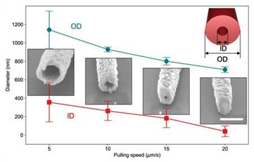
The researchers explain that steering the crystallization in three dimensions is based on moving the nanopipette with a motorized stage (see video below): "When an ink-filled nanopipette with a diameter of 600 nm approaches and physically contacts a Si substrate, fL-volume ink is wetted on the substrate, forming the meniscus at the pipette–substrate gap. CH3NH3PbI3 crystals immediately start to grow inside the ink meniscus." "As the pipette moves up (or the substrate moves down) with a constant pulling speed, the crystal growth is guided in three dimensions with the continuous ink supply from the pipette," they describe the 3D-printing process. "The termination of the growth is conducted by abruptly increasing the pulling speed above a threshold speed, enabling in situ tailoring the dimensions of a freestanding perovskite nanowire." The pulling speed is a central factor to control the perovskite nanowire growth. Furthermore, the accurate pulling process can control the nanowire's internal structure (see figure below). The evaporation-driven transport of perovskite solutes is dependent to the meniscus size controlled by the pipette pulling. Specifically, the hollowness of perovskite nanowires from tubular to solid shapes can directly be controlled by instant variation of the pipette pulling speed.  Growth dynamics of 3D-printed perovskite nanowires. The internal structure of a perovskite nanowire can also be tuned by ν. As ν increases, the internal structure changes from hollow to solid shapes due to decrease in the inner diameter, ID. Both OD (circle) and ID (square) decrease as ν increases at 50% RH. Inset: FE-SEM images showing cross-sections of perovskite nanowires obtained from different pulling speeds (scale bar: 1 µm). Reprinted with permission by Wiley-VCH Verlag
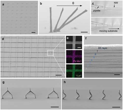
Production of mesh-shaped structures is a primary step toward layer-by-layer additive manufacturing process and by lateral guiding an ink meniscus using a nanopipette with 90° tilting the researchers demonstrated the reliable fabrication of perovskite mesh structures.
 3D perovskite architectures. a) An array of vertical perovskite nanowires (scale bar: 20 µm). b) Tilted perovskite nanowires fabricated by varying the pipette–substrate angle (scale bar: 5 µm). c–e) Fabrication of mesh structures. c) Optical microscopy images showing the horizontal printing process by tilting the pipette 90°. d) FE-SEM image of a perovskite mesh structure (scale bar: 20 µm). e) Magnified FE-SEM and EDX images of a perovskite nanojunction (scale bar: 1 µm). f) A perovskite nanowall consisting of stacked eight layers (scale bar: 1 µm). g) Freestanding arc-like junctions (scale bar: 10 µm). h) Vertical serpentine structures (scale bar: 10 µm). Reprinted with permission by Wiley-VCH Verlag
By Michael Berger – Michael is author of three books by the Royal Society of Chemistry: Nanotechnology: The Future is Tiny, and Nanoengineering: The Skills and Tools Making Technology Invisible NW. Posted: Feb 11, 2020. |
|||||||||||||||||||||||||